


What is Nano?

Image adapted from L. S. C. Pingree, M. C. Hersam, M. M. Kern, B. J. Scott, and T. J. Marks, "Spatially resolved electrolumines-cence of operating organic light-emitting diodes using conductive atomic force microscopy," Appl. Phys. Lett., 85, 344, 2004.
Over the past decade a new term has entered our vocabulary and that word is "nano." We hear the word in movies. It's mentioned on television and in newspapers and magazines. Futurists say it will pave the way for unimaginable new possibilities. Pessimists are unsure.
There are many different opinions about where this new field will take us, but everyone agrees that this science and the new technologies that come from it have the possibility of significantly impacting our world.
This introduction will provide some basic information to help you understand not only what nanotechnology is,but what it isn't.
The Beginning

This is how nano is represented mathematically. Ten to the negative 9th equals one billionth or 1/1,000,000,000.
To begin, "nano" is actually a prefix that comes from the Greek word for dwarf.
It simply means one billionth. So, one nanometer (1 nm) is one billionth of a meter.
There are three important "nano" terms to consider when you're trying to understand the increasing news coverage and scientific developments in the field of nanotechnology. These terms are: Nanoscale, Nanoscience and Nanotechnology.
A Word on Measurements
© Royalty-Free Corbis
Scientists and much of the world outside of the United States measure mass, length, and volume using the metric system. We will be using this system throughout the site.
Here is a list of metric measures to help those who are not familiar with this system.
| Unit | Abbreviation | Description |
|---|---|---|
| meter | m | apporoximately three feet or one yard |
| Centimeter |
 m m |
1/100 of a meter, about half of an inch |
| millimeter | mm | 1/100 of a meter |
| micrometer | m |
1/1,000,000 of a meter, often called a micron-most integrated circuits are at this scale |
| nanometer | nm |
1/1,000,000 of a meter, the size of a single molecule |
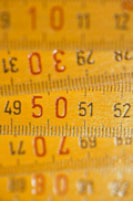
How Small is Small?

This is Nanoscale objects have at least one dimension (height, length, depth) that measures between 1 and 999 nanometers (1-999 nm). *Images © Dennis Kunkel Microscopy, Inc.
As stated previously, a nanometer is one billionth of a meter. Everyone struggles to imagine this very small scale, but you can get an idea through comparison.
Let's look at some commonplace objects. Pick up a book and look at the thickness of an individual page. The average page is about 100,000 nanometers thick. Remember, to be considered nanoscale the object must have one dimension between 1 and 999 nanometers, so this is definitely not within the nanoscale range. A very fine human hair is about 10,000 nanometers wide, which is the smallest dimension we can see with the naked eye.
Although technically nanoscale objects are within the 1-999 nm range, often when people refer to something as being "at the nanoscale," they are speaking about objects smaller than 100 nanometers. Why? When nanoparticles are in the 1-100 nm size scale, usually.
Size Matters!
When objects are below 100 nanometers in size they can exhibit unexpected chemical and physical properties.
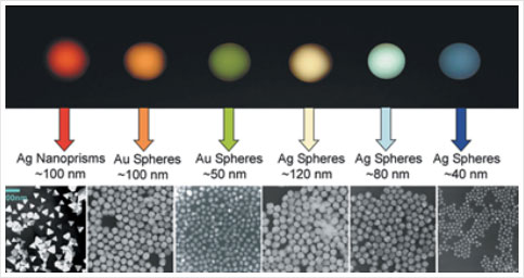
For example, you could cut a block of gold into smaller and smaller pieces and it would still have the same color, melting temperature, etc. But at certain ranges of the nanoscale, gold particles behave differently. The image below shows how gold nanoparticles of different shapes and sizes are different colors.
The chemical properties (reactivity, flammability, etc.) and the physical properties (melting point, conductivity, etc.) can all change at the nanoscale. So, the properties are dependent on the size of the material. Size-dependent properties are the major reason that nanoscale objects have such amazing potential.
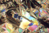
Nanotech Instruments
© Northwestern University (courtesy M. Hersam)
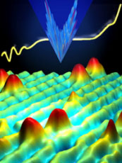
We know nanostructures exist in the same way that we know that molecules exist - with the aid of specialized instruments.
Molecules with more than 10 atoms fall into the nanometer range. Scientists were not able to visualize individual molecules and nanoscale objects until the invention of some very powerful microscopes. These microscopes don't use light to create an image of a nanoscale object.
Believe it or not, waves of light are too large - visible light has a wavelength between 400 and 750 nanometers. That's much larger than many nanoscale objects and definitely larger than most molecules. Instead the specialized microscopes use very small probes or electrons.
With these microscopes, a very small, very sharp tip on the end of a lever is dragged across a nanoscale object. The movement of the lever is monitored with a computer, which creates an image. The method is much like a person moving their fingers over words written in Braille to read. This tip-scanning method is known as Scanning Probe Microscopy (SPM). Electron microscopes are similar to light microscopes except instead of directing light to a sample, they direct electrons to the sample.
Size-Dependent Properties

© Northwestern University (courtesy M. Hersam)
While microscale objects (objects with dimensions one-millionth of a meter in size) are widely used, they haven't caused the same excitement as nanoscale materials. The reason is that microscale objects have essentially the same properties as bulk material. However, at the nanoscale the fundamental properties of materials depend on their size, shape, and composition in a way that they don't at any other scale. So, the nanoscale is a different kind of small.
Size-dependent properties are the reason that nanoscale objects have the potential to significantly impact both science and industry.
Examples of size dependent properties include:Catalytic properties - how the material enhances chemical reactions Electrochemical properties - how the material transfers electrons to other chemical constituents Melting properties - how the material transitions from solid to liquid Magnetic properties - how the electrons interact to induce magnetic poles Optical properties - how the material interacts with light (e.g., its color) It is difficult to predict at what size a particular material will transition from bulk to size-dependent properties. This threshold is different for each material and each property. For example, nanoscale gold will have different colors throughout the nanoscale size range, but the size-dependent catalytic properties do not dramatically change until gold features are smaller than five nanometers.
Building Methods
© Northwestern University (courtesy C.A. Mirkin)
© Northwestern University (courtesy S.I. Stupp)
There are two general approaches to building structures. These methods are called top-down and bottom-up. Using top-down methods, researchers selectively modify the starting material much like an artist creates a sculpture from a slab of marble. This method is more traditional in that material is altered (e.g., removed, added to, etc.) by mechanical or chemical means. Photolithography and electron beam lithography are examples of top-down approaches that are used extensively in the semiconductor industry to fabricate integrated electronic circuitry.
Some top-down approaches are already well developed and being commercialized. There are some who believe that there are limits to this method.
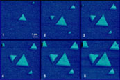
Using the bottom-up method, researchers seek to build larger and more complex systems molecule-by-molecule. With this method, molecules are designed and created that have the ability to spontaneously self-assemble when a chemical or physical trigger is applied. Nature routinely uses this method. Although bottom-up processes are less developed and understood, they hold great promise for the future.
At the nanoscale, researchers are working at both ends of the spectrum and these two general approaches are converging.
Bringing it All Together

© Northwestern University (courtesy Clifton Shen)
Once the size-dependent properties of a particular material are discovered, they may open the door for new ways of using the material. New applications also become possible because nanoscale items are so small that they can often be placed into an environment (like the human body) without harming it. Using the special properties that occur at the nanoscale to develop new technologies is called nanotechnology.
The field of nanotechnology focuses on three main areas: Developing new tools to measure, and new chemistry to make, highly miniaturized structures. Identifying the chemical and physical changes that occur at the nanoscale. Using the chemical and physical changes that occur at the nanoscale to develop new technologies. Nanotechnology gives us an entirely new way to make and study materials and devices in all fields of science and engineering. The exploration of nanotechnology is going on around the world and includes researchers from many different fields including chemistry, physics, material science, engineering, biology, and medicine. Several commercial examples of nanotechnology are on the market, and many more promising applications of nanotechnology are being investigated.